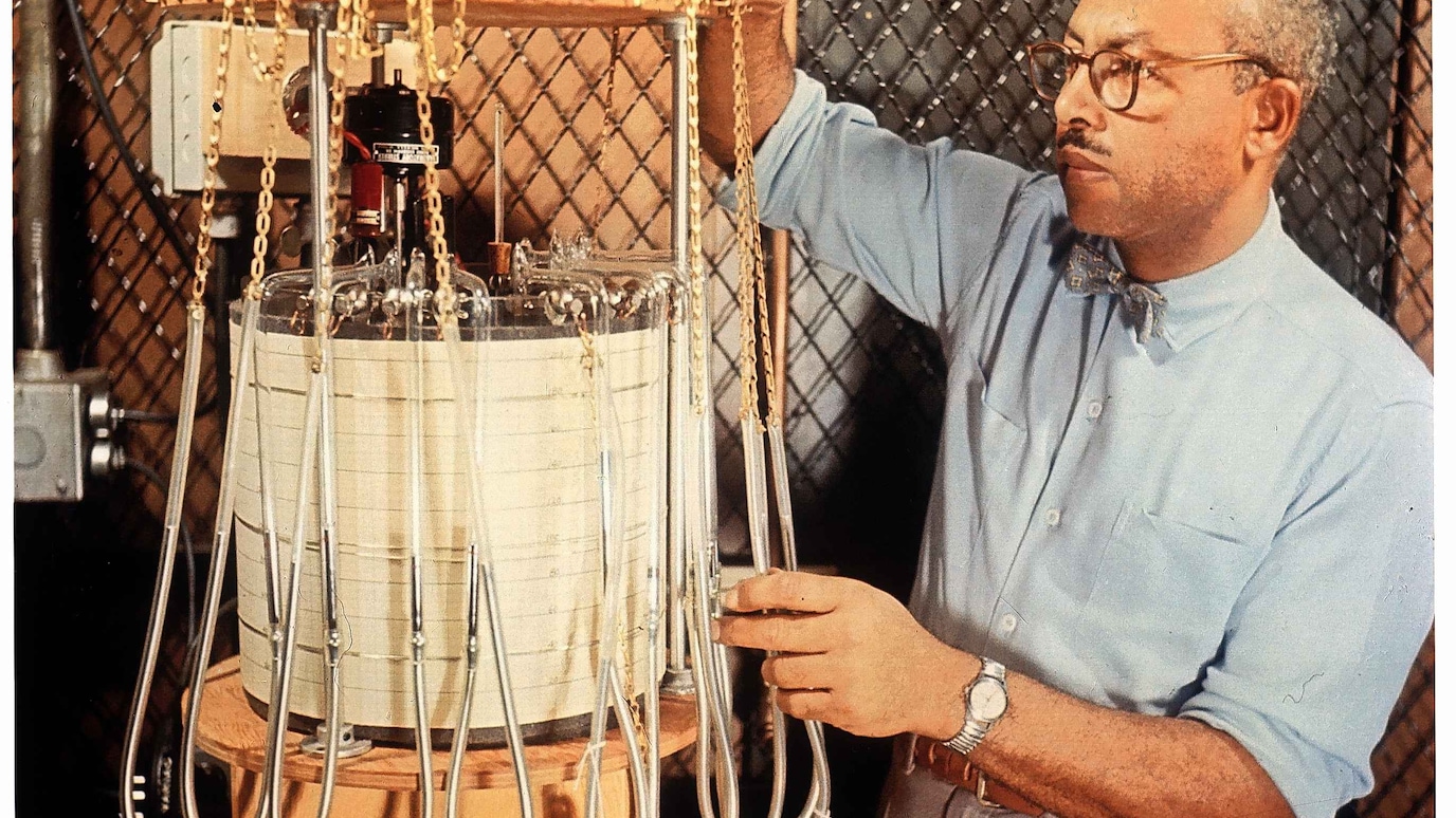
This article follows a previous one published in Volume 41/3 1966 of this magazine.
We analyze the performance of different handoff algorithms for the forward link or downlink of a CDMA cellular system.
Load balancing provides a key mechanism for achieving efficient resource allocation in data centers, ensuring high levels of server utilization and robust application performance.
Reconfigurable intelligent surfaces (RISs) have emerged as one of the most promising techniques for future 6G wireless networks.
We demonstrate a chirp-free optical pulse generator using a phase modulator and a delay interferometer.
We consider the problem of power control for mobile data users with an average power constraint.
Statistical multiplexing of video content aims at transmitting several variable bit rate (VBR) encoded video streams over a band-limited channel.
The cellular network evolution has generally focused on improving system and edge user throughput while reducing latency.
In this paper, we propose a TDMA based simple transmission scheme, which overcomes the effect of the delays caused by the poor synchronization of the relaying nodes over Ricean channels.
The decomposition of methane under ion bombardment is a model for decomposition of more complex molecules and polymers.
Explore more

White paper
Video
AI-enhance wireless reliability: joint source and channel coding for robust 6G air interface

Blog

Blog
